Cutting-Edge Memory Solutions
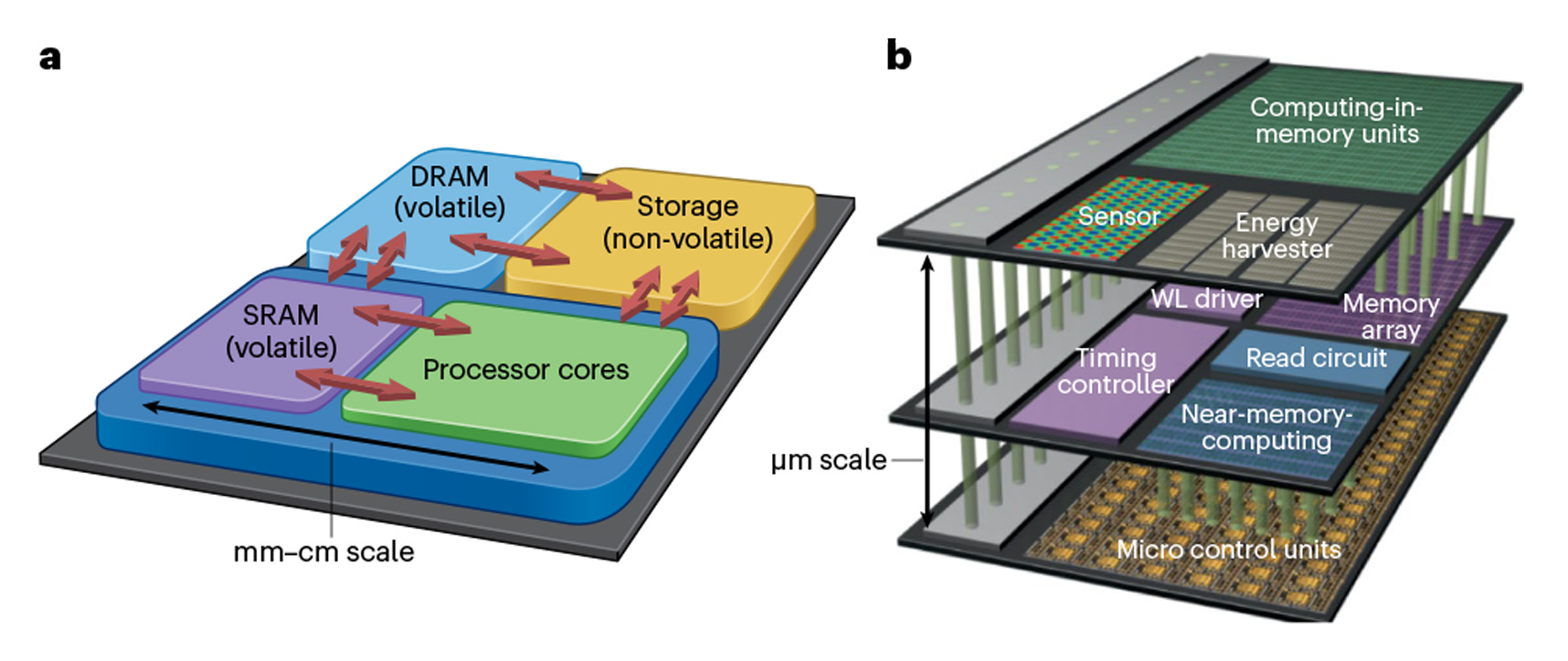
Comparisons of current versus vertical memory integrated computer architectures
- Schematic of a conventional von Neumann computing architecture that is subject to memory bandwidth limitations due to processing and memory units such as SRAM, static RAM and DRAM, dynamic RAM being physically separated by distances of millimetres to centimetres.
- Conceptual diagram of an advanced 3D monolithic memory and sensor integrated microprocessor chip enabling near- and in-memory computing applications. A key advantage of this architecture is the micrometre-scale physical distances between memory and processing units, permitting high-bandwidth access for big data computing applications.
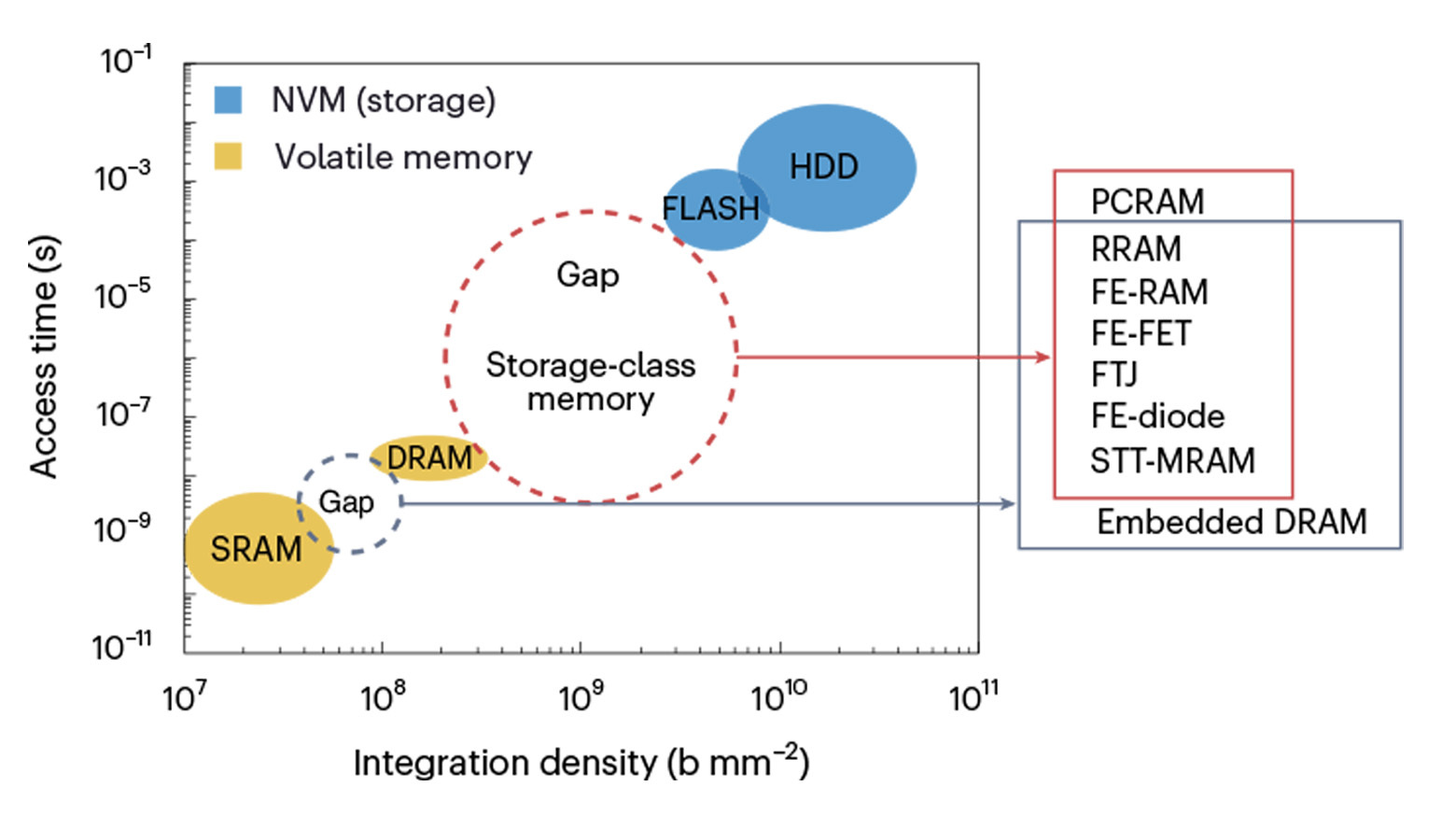
Comparison of access time versus integration density (in bits/mm2) for various volatile memory and NVM technologies
The prominent performance gap between storage-class NVM and volatile working memory can probably be filled by emerging NVM technologies such as resistive RAM (RRAM), phase change RAM (PCRAM), spin-torque transfer magnetic RAM (STT-MRAM), ferroelectric (FE) tunnel junctions (FTJs), FE-RAM and FE field-effect transistors (FE-FETs). The size and speed gap between volatile SRAM and DRAM technologies could also be addressed by these emerging NVM technologies.
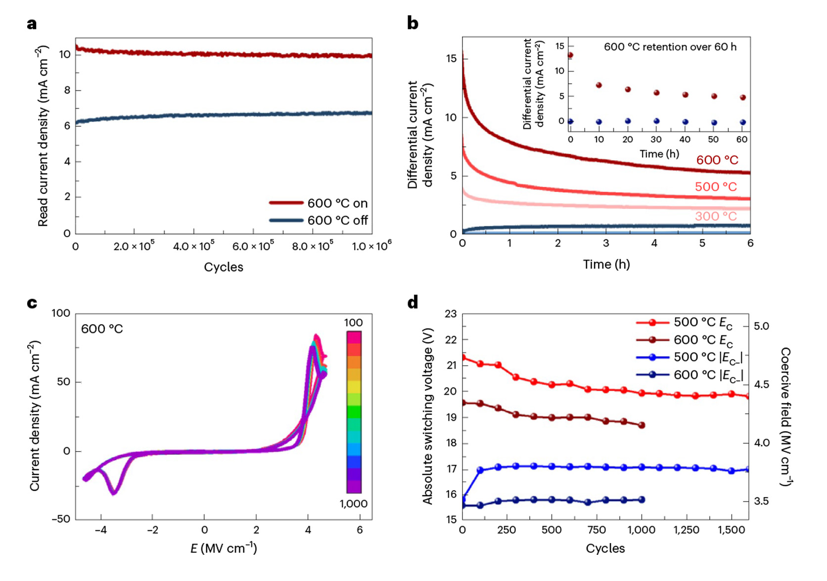
Ferrodiode read and write endurance and retention performance
- More than 1M read endurance cycles at 5 V read voltage 600°C.
- The retention behaviour at 5 V read voltage at 300, 500 and 600°C (inset) and the retention behaviour at 5 V read voltage at 600°C over 60 h.
- Triangle wave I–V survival tests during 19 V write cycling at 600°C.
- Positive and negative switching voltages from test triangle wave I–V versus the number of write cycles at 500 and 600°C.
General Structure of the AlScN FE Diodes
The FE diodes in this work consist of 50 nm thick Al bottom electrodes grown on a sapphire wafer. The ferroelectric layer consists of sputter-deposited 5, 10, or 20 nm thick Al0.72Sc0.28N/Al0.64Sc0.36N. The IL consists of ALD-deposited AlOx with thickness ranging from 0 (no IL) to 5 nm. The top electrode arrays consist of 20 μm-radius pads of Ti or Cr metal with a Au capping layer. The detailed information on the fabrication processes is described in the Methods section. TEM images of our devices are shown in Figure below:
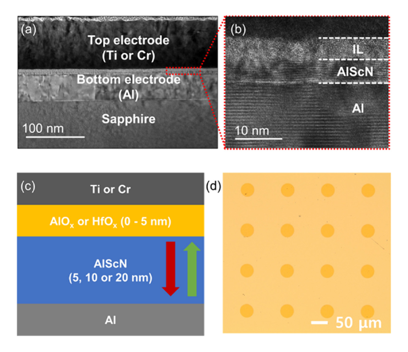
- Cross-sectional bright-field STEM and
- high-resolution TEM image of the device.
- Schematic diagram of the MFIM Al0.72Sc0.28N/Al0.64Sc0.36N ferroelectric diode.
- Optical image of the device array. The darker contrast circles represent the top metal electrodes of 20 μm radii.
Reconfigurable Compute-In-Memory on Field-Programmable Ferroelectric Diodes
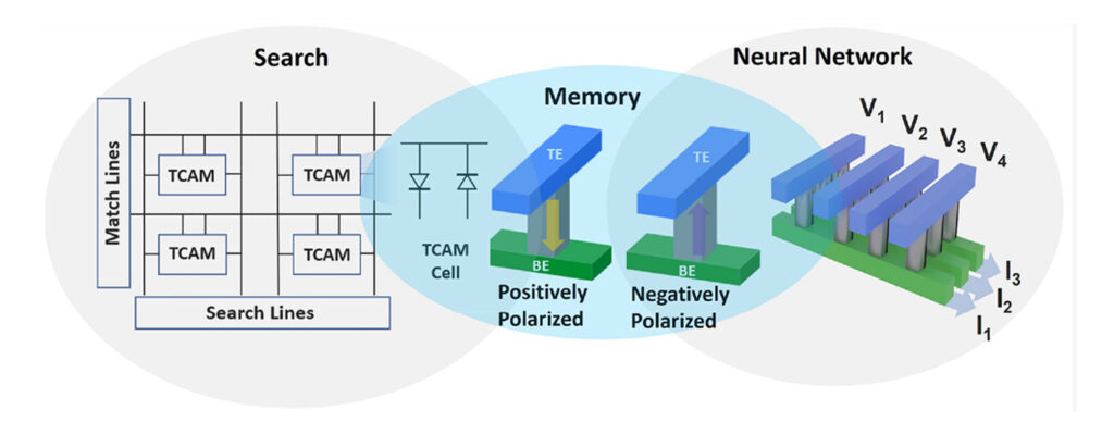
The deluge of sensors and data generating devices has driven a paradigm shift in modern computing from arithmetic logic centric to data-centric processing. Data-centric processing requires innovations at the device level to enable novel compute-in-memory (CIM) operations. A key challenge in the construction of CIM architectures is the conflicting trade-off between the performance and their flexibility for various essential data operations. Here, we present a transistor-free CIM architecture that permits storage, search, and neural network operations on sub-50 nm thick Aluminum Scandium Nitride ferroelectric diodes (FeDs). Our circuit designs and devices can be directly integrated on top of Silicon microprocessors in a scalable process. By leveraging the field-programmability, non-volatility, and nonlinearity of FeDs, search operations are demonstrated with a cell footprint <0.12 μm2 when projected onto 45 nm node technology.
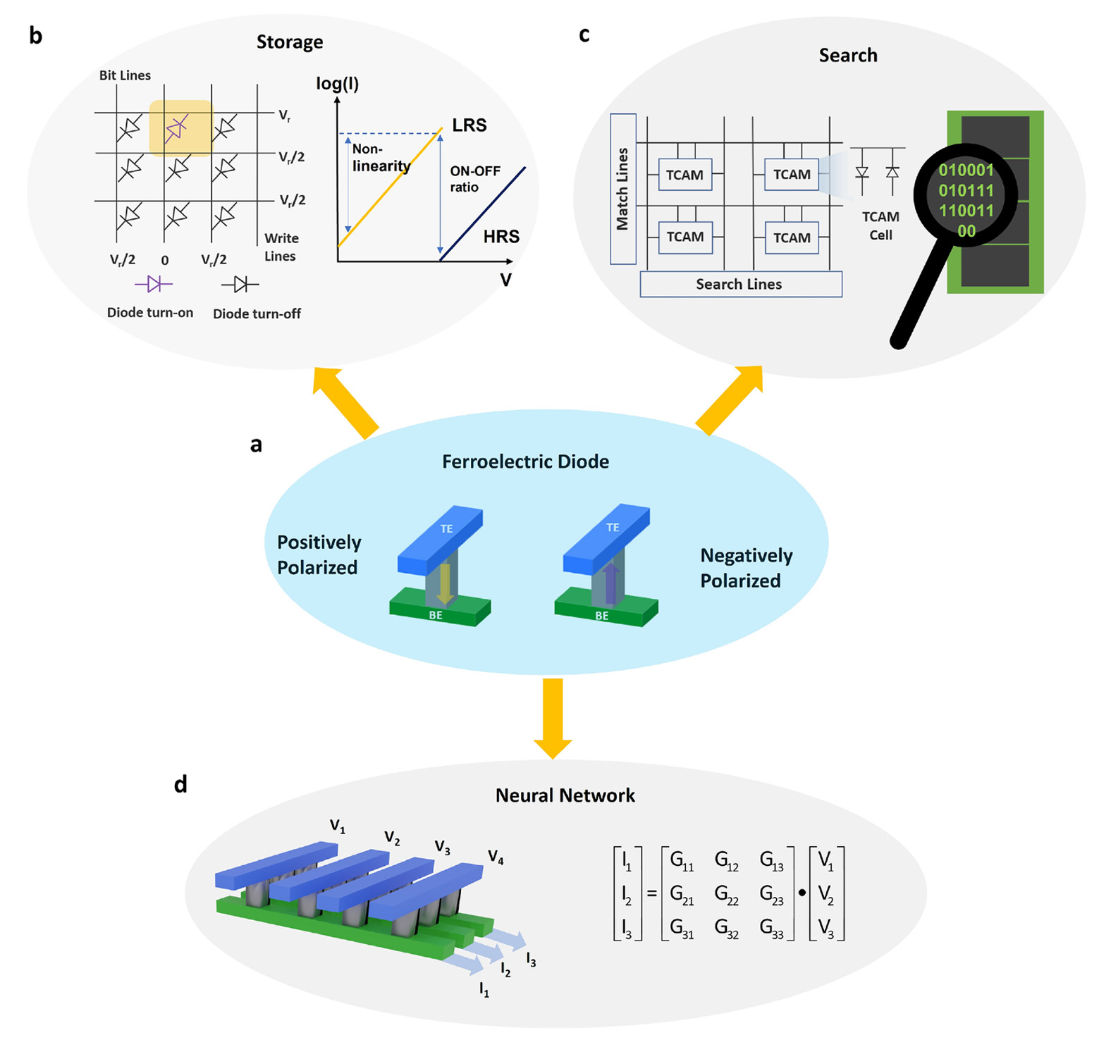
- Schematic diagram of FeD devices in a cross-bar structure with up and down polarization of the ferroelectric AlScN. The field programmability, non-volatility, and nonlinearity of these devices can be leveraged for multiple, primitive data operations such as storage, search, and neural networks without the need for additional transistors, as shown in (b)−(d).
- The two-terminal FeD devices show a diode-like self-rectifying behavior with nonlinearity >106 concurrently with an ON/OFF ratio over 102 and write-endurance over 104 cycles, making FeD devices well placed in the memory hierarchy for storage. Due to the high coercive field of AlScN, the read-disturbance would also be minimized which will result in high read-endurance. In addition, the high nonlinearity can suppress sneak currents without the need for additional access transistors, or selectors.
In addition, the high nonlinearity can suppress sneak currents without the need for additional access transistors, or selectors. - For search operations, a nonvolatile TCAM can be built upon 0-transistor/2-FeD cells, which serves as a building block in hardware implementation of in-memory computing for parallel search in big data applications.
- For neural networks, FeD devices can provide programmability to distinct multiple conductive states with a high degree of linearity with respect to a number of electrical pulses. This allows mapping the matrix multiplication operation, a key kernel in neural-network computation, into reading the accumulated currents at each bitline of a FeD device by encoding an input vector into analog voltage amplitudes, and the matrix elements into conductances of an array of FeD devices. The matrix multiplication operation is benchmarked by mapping neural network weights to experimental FeD conductance states in a convolutional neural network architecture for both inference and the in situ learning task, and shows that our accuracies approach ideal software-level simulation on the MNIST data set.